SEMI CONDUCTOR CONTENT

INTRODUCTION
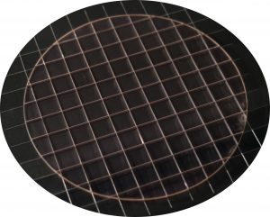
DOE are used in many semi conductor applications, mostly in the UV and visible wavelengths. Our high grade UV fused silica DOE give unparalleled performance stability for direct writing lithography applications and wafer metrollogy applications common in the semiconductor industry. In these precise applications, our DOE provide superior performance due to the almost absolute angular accuracy , excellent thermal stability and high laser damage threshold
For more information, please contact [email protected].
Wafer Inspection
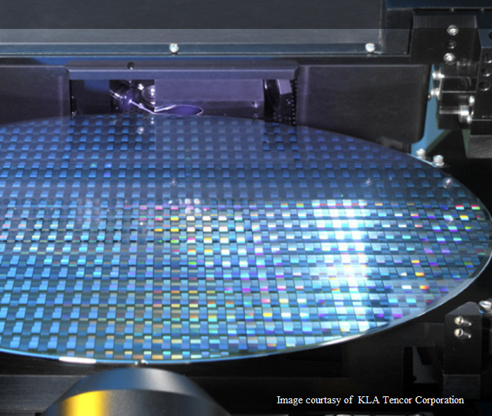
As the ITRS2 drives the semiconductor industry to greater miniaturization, there is an increasing need for the development of DUV wafer inspection systems capable of resolving such features. These systems require shaping of the light- either by diffusers (for low coherence sources) or by beam shapers (for highly coherent single mode laser sources). The illumination is also often done at high grazing angles (>70 degrees), requiring careful design of the shaping optics to achieve high uniformity on the wafer surface.
Holo/Or has some unique solutions for the wafer inspection field, including custom beam shaping elements and modules that can achieve high angle uniform shapes at high grazing angles.
Relevant products: Beam Shapers, collimated beam shaper, diffuser

Direct Laser Lithography
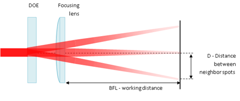
Many applications in the semi conductor industry require high throughput direct laser writing of multiple lines. these include flat display mask writing, solar panel electrodes writing and other multi-line exposure processes. For these applications, our high quality beam splitter DOE offer unparalleled precision and uniformity, eliminating line thickness variation and enhancing throughput.
Relevant products: Beam Splitter 1D


