Enhancing Laser Metrology with Diffractive Optics: Precise Solutions for Semiconductor Manufacturing
Home » Enhancing Laser Metrology with Diffractive Optics: Precise Solutions for Semiconductor Manufacturing
12:13 PM
Introduction to laser Metrology applications
Laser metrology, an important technique in semiconductor manufacturing, relies on precise optical measurements to ensure product quality and yield. Laser metrology refers to a wide array of techniques that utilize lasers to measure physical dimensions of parts or sub-parts (such as microstructures on a wafer).
Diffractive optics, with their unique properties, offer significant advantages in enhancing the performance and efficiency of laser metrology systems. A variety of industries utilize laser optical metrology due to the undeniable advantages it offers, as detailed in the below table:
Industry
Application
Some key advantages per industry
1
Semiconductors
In fabrication, it is used for characterizing micro-structures and complex geometries e.g. optical critical dimension (OCD).
High Precision and throughput, non-destructive
2
Aerospace & Automotive
Laser metrology is used to measure critical components with High precision
Traceability that meets the highest standards
3
Medical
Enhancing manufacturing of medical devices by measuring physical dimensions
Measures quickly and accurately
Table 1: Laser metrology key benefits per Industry segment
Laser Metrology usage in the Semiconductor Industry
Laser metrology equipment, such as laser interferometers, is used to passively scan and characterize substrates, making this non-destructive optical method superior to others. Furthermore, laser scanning metrology offers high sensitivity, precision, and accuracy, which is why it is widely adopted by leading semiconductor industry players. The quality of each device is governed by the performance of the fabrication machinery and its tight process control.
Semiconductor fabrication facilities prioritize yield and throughput, driving the integration of wafer inspection tools into production lines. These tools provide real-time 3D data for process optimization, enabling the characterization of nanometric features, roughness, wafer bow, film thickness, and defect inspection. The result of high-precision machinery is high-quality device and consequently, a high-quality consumer product.
Challenges in Laser Metrology
Accurate laser metrology requires state-of-the-art components to minimize noise and ensure precision. High-resolution measurements, especially for features created using extreme ultraviolet lithography, demand advanced optical solutions.
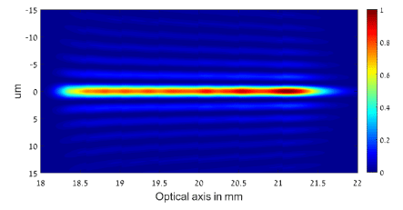
Laser metrology scanning may be used to measure small features created by extreme ultraviolet lithography , a cutting-edge lithography technique used to create extremely small features in semiconductor devices. Such laser metrology can employ elongated focus DOEs to improve resolution and increase the detection range. An illustration of elongated focus produced by Holo/Or’s diffractive optics can be seen below:
Diffractive Optics: A High Precision Solution for laser metrology
Holo/Or’s Diffractive Optical Elements (DOEs) offer a range of benefits to laser metrology applications:
High Precision: Tight tolerances and near-absolute angular accuracy ensure precise measurements.
Customization: Tailored field of illumination, from lean-line to uniform top-hat, meets specific requirements
Design Support: Holo/Or offers simulations of our DOEs performance in with customer supplied optical systems
Durability: Our DOEs are etched, monolithic fused silica or Zinc selenide window with laser grade AR coating. They have high LDT, high stability and no polymers or other soft materials.
Holo/Or specializes in beam shaping and splitting solutions, including collimated beam shaping elements, diffractive prism arrays, diffractive lens arrays and diffractive beam splitter elements. These elements can be combined into a single component incorporating multiple optical functions in a single surface and reducing interference due to back reflections.
An illustrated flat top line generated from Gaussian beam using Holo/Or’s Diffractive Optics
Conclusion
Diffractive optics, integrated into laser metrology systems, can boost system performance and speed in semiconductor manufacturing. By offering precision, durability and customization, these elements enhance defect inspection, metrology, and lithography processes. Holo/Or’s expertise in diffractive optics provides tailored solutions that meet the demanding requirements of the semiconductor industry, including a full support envelope with simulations of our components in the customers optical setup. Check out our custom solutions, and feel free to contact us for more details
TL; DR – Q&A SUMMARY
What are diffractive optical elements?
Diffractive Optical Elements (DOEs), are optical components that utilize microstructures to manipulate light waves. Unlike traditional refractive optics, DOEs alter the phase of light, enabling the creation of complex light patterns that would be difficult or impossible to achieve with conventional methods. These versatile elements offer advantages in terms of size, precision, and functionality, making them ideal for various applications in optics and photonics.
Why are Diffractive optical elements used in laser metrology and other inspection systems?
DOEs demonstrate exceptional precision, making them well-suited for demanding applications in laser metrology and other inspection systems. Holo/Or's expertise allows for the integration of multiple optical functions into a single DOE, and the manufacturing of elements with distinct sub-apertures, each serving a specific purpose. This capability is particularly valuable for correcting deflection angles or aberrations.
what are the requirements for using diffractive optics in semiconductor manufacturing machinery?
To ensure optimal performance in semiconductor laser machinery, DOEs should be integrated in a correct position within the optics. For most systems, this position is before the focusing optics. Furthermore, beam size should be <X2 clear aperture for beam shaper DOEs , to enable uniform shaping.
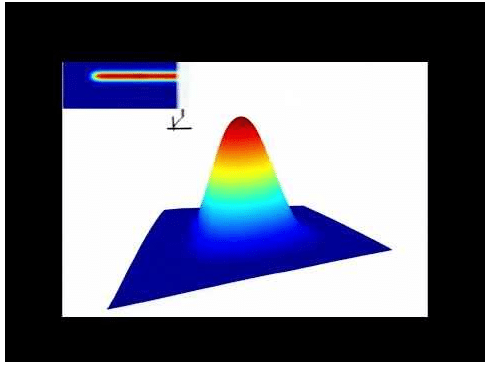 An illustrated flat top line generated from Gaussian beam using Holo/Or’s Diffractive Optics