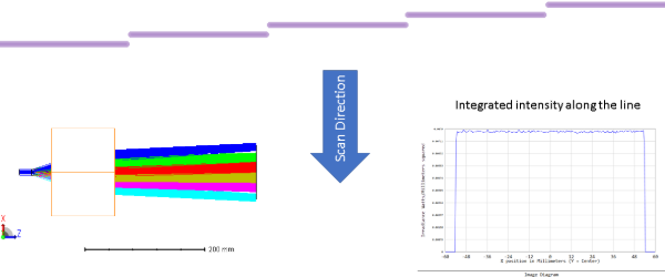
Laser de-bonding requires the formation of a thin long line, typically achieved by using large complex and expensive cylindrical optics. This article presents an alternative approach utilizing a single DOE and a standard F-theta lens.
Background: laser UV debonding
In many flat panel processes, the active screen layer is often extremely thin, making processing extremely challenging. To deal with this issue, the layers are often bonded with a special adhesive to a carrier wafer for ease of processing. Following this bonding and processing, the active layers must be de-bonded from the carrier wafer, either through a chemical process, a mechanical process or, as is becoming more and more common, by laser debonding. Laser UV de-bonding being the cleaner, more economic and more ecologic method than the alternatives, and is rapidly becoming a leading de-bonding method in flat panel display production.
Often, to perform the laser de-bonding process, a long thin line of UV laser energy is scanned over the wafer, to achieve high rate and good uniformity of de-bonding without damaging the screen layer. The typical thickness of such lines is between 20-50um and its lengths 100mm or more. To achieve such lines dimensions, a large cylindrical optics is normally used, however – such optics is difficult to produce, mount and align.
This article presents an alternative method to obtain similar results by using a single custom DOE (Diffractive Optical Elements) in combination with a single mode UV laser and a standard F-theta scan lenses, to generate uniform integrated line intensity scanning over lines of up to 100mm.
Diffractive Optical Element basics
A diffractive optical element is a transmissive phase mask that can impose any arbitrary phase on the wavefront of the laser passing through it. This phase changes the beam intensity at the far field, enabling the diffractive optical element, often called a diffractive lens, to shape the beam or split it. A custom diffractive optical element can be designed to provide any desired intensity distribution at the focus of the system (which is the far field), including a combination of splitting and flat top line shaping functions, for example. The diffractive optical elements market is highly diverse, as they are used in many laser applications, such as material processing, aesthetic medicine, metrology, AR/VR and others.
Diffractive optics design, fabrication and test
DOE design employs advanced computer aided methods such as iterative Fourier transforms to optimize the phase of the custom diffractive optical element so that it generates the desired intensity distribution. Following the phase design, the custom diffractive optical element is produced by semiconductor methods, where the phase profile is lithographically written and etched.
Following production, diffractive optics for industrial and commercial applications must be individually tested to verify the performance since often, they are employed in high-value, high-powered laser systems where non-conformance can risk damage to other system components. This testing is done both optically and topographically (to verify that the produced phase is as planned).
Custom diffractive optical element as a de-bonding line generator without cylindrical optics
It is possible to generate a highly uniform flat-top UV line by using a custom diffractive optical element and an F-theta focus lens however, manufacturing tolerances limit the DOE beam shaper angles so that for all commercially available scan lenses, such lines are no more than 20mm long.
An effective way to overcome this limit is by adding a second DOE during the process development stage, a 1-dimensional diffractive beam splitter. The beam splitter is rotated at a slight angle so that the split lines that are formed are arranged in a staircase like manner, with overlap controlled by the rotation angle. By adjusting the rotation of the custom diffractive optical element, the stitching can be accurately controlled, resulting in a scanned line that is uniform over the entire field of the F-theta i.e., more than 100mm.

Once the correct angle is found, both DOEs can be combined in design into a single custom diffractive optical element that will generate the lines staircase. Thus, a high uniformity line of 100mm can be generated by using a single mode UV laser, a single DOE and an F-theta lens, without the need for large, high quality cylindrical optics and an anamorphic system. This approach offers an easy to align, elegant and cost-effective.
TL; DR - Q&A summary
What is UV laser debonding?
Laser debonding is a process where a thin layer is separated from a carrier wafer by applying high laser UV intensity to it, often shaped as a thin (<50um), long line of 100mm length or more, requiring large cylindrical lenses.
How can diffractive optical elements help with laser de-bonding?
By using a single mode UV laser with a line beam shaper and a multi-spot diffractive beam splitter, and focusing the resulting beams using a standard F-theta lens, it is possible to generate a perfectly stitched line of over 100mm length and diffraction limited thickness, without any cylindrical optics. Once the correct rotation for perfect stitching is found, the two DOE can be combined into a single custom diffractive optical element.
How do DOEs work?
DOEs are transparent windows that manipulate the phase of a laser beam by creating variable delays at different areas. This is done by etching the glass into different heights at different points on the DOE surface.
How are DOEs designed, produced and tested?
The design of each custom diffractive optical element is done with computer-based tools that define the optimal phase profile, taking into account production tolerances. The phase is then produced using semi-conductor methods, and the element is tested using an automated optical setup, as well as topological measurements.

